Chapter 10 Vendor: STM32
The following chapters provide descriptions and examples for STM32 microcontrollers. All chapters so far tried to be as vendor agnostic as possible. The following sections only apply to STM32.
This chapter is stuctured as follows:
- Section 10.1 provides an overview and introduction on that the Bluepill evaluation board is and how it can be used.
- The Bluepill board is used in previously for example in the chapter about how to use a Logic Analyzer: Example 1: UART
- Section 10.2 provides an overview and introduction on the STM32L5, including its TrustZone capabilities.
- Section 10.3 provides TrustZone-enabled firmware examples for the ST32L5.
10.1 STM32 “Bluepill” STM32F103C8T6
The Bluepill is pretty popular and very cheap development board equipped with a STM32F103C8T6 microcontroller.
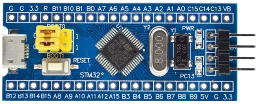
Figure 10.1: The Bluepill board
You can find the datasheet on st.com.
More on Bluepill:
10.1.1 Hardware Overview
- Microcontroller: STM32F103C8T6
- Arm Cortex M3 at 72 MHz
- 64 Kbytes Flash
- 20 Kbytes of SRAM
The microcontroller supports all the basic embedded communication protocols:
- UART / USRT / LIN: 3
- I2C: 2
- CAN: 1
- USB: 1
On reblag.dk you can find the following pinout diagram:
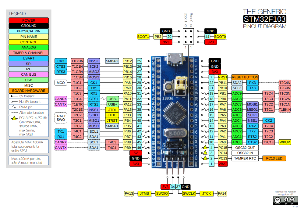
Figure 10.2: Pinout Diagram (source: [9])
10.1.2 Memory Map
The full memory map can be found in the datasheet. [10]
| Region | From..To | Description |
|---|---|---|
| Aliased to Flash or system memory | 0x0000 0000 .. 0x0800 0000 |
Aliased to either Flash Memory or system memory
depending on the BOOT0 and BOOT1 configuration. See 10.1.3 |
| Flash memory | 0x0800 0000 .. 0x0801 FFFF |
Flash - what you program. |
| System memory | 0x1FFF F000 .. 0x1FFF F800 |
System Memory contains the boot loader. |
| Option Bytes | 0x1FFF F800 .. 0x1FFF F80F |
Here you can define read out protection or write protection for Flash. See 10.1.5 |
| Peripheral | 0x4000 0000 .. 0xFFFF FFFF |
Peripherals and Cortex-M3 internal Peripherals. |
10.1.3 Boot Modes and Programming
The microcontroller offers three boot modes, which are selectable via the BOOT-Pins. These pins BOOT0 and BOOT1 are conveniently available as jumper pins. As you can see in the pinout diagram or in the picture below, you can select 0 or 1 easy by settings the jumpers accordingly.
- If you have
BOOT0at 0, you will always boot from main flash memory. - If you have
BOOT0at 1 andBOOT1at 0, you will boot into the boot loader, which is programmed into the system memory. - If you have
BOOT0at 1 andBOOT1at 1, you will boot into embedded SRAM.
There are multiple ways to program the main flash memory. As almost all STM32 devices a UART interface is available, when the device is booted into the boot loader. To boot into boot loader, set BOOT0 to 1 and BOOT1 to 0.
Then you can program the device either via SWD or JTAG. See @ref(#bluepill-db) for details on how to connect to these ports.
10.1.4 Debugging
If you want to use SWD or JTAG to program a device, you can leave BOOT0 and BOOT1 at 0 and boot into main flash memory. Altough, if you used the STM32CubeIDE to generate a bare metal firmware and did not any special configuration for the pins PA13 and PA14, the SWD and JTAG ports are disabled by default and those pins are available as GPIO ports. This means you won’t be able to program the device via JTAG or SWD. Specifically, JTAG and SWD are disabled in HAL_MspInit() via the macro __HAL_AFIO_REMAP_SWJ_DISABLE.
An easy workaround is to boot into boot loader mode and program the microcontroller there - ie. set BOOT0 to 1 and reset the device. In boot loder mode JTAG and SWD are available.
You can also enable the SWD interface in the MX Editor in the “System Core” -> SYS -> Debug configuration section.
For Debugging the STM32F103C8T6 provides JTAG and SWD. As you can read in the Reference Manual ([11]) the STM32F103xx provides a standard Arm CoreSight debug port, which is 5 pin JTAG and a 2 pin Serial Wire (SWD) debug port. In CoreSight JTMS from JTAG and SWDIO from SWD and as well as JTCK and SWCLK are multiplexed together.
The pins for SWD (SWCLK, SWDIO) are available as separate pins on the board:
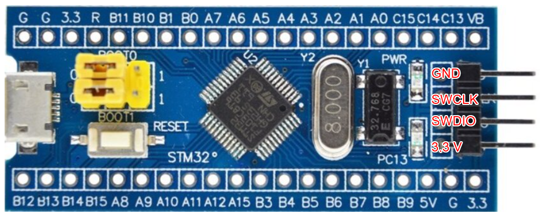
Figure 10.3: SWD port on the Bluepill
To connect to these ports you can use a cheap ST-Link debugger and programmer. There are very cheap ones available, just search for “ST-Link v2.” I have the following device:
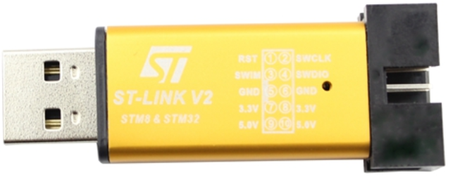
Figure 10.4: Cheap ST-Link v2 programmer and debugger
You will need 4 female to female jumper cables, hook them up to the correct pins as they are labeled on the ST-Link and your Bluepill and go.
10.1.5 Read out and write protections
The STM32F103C8T6 provides only very simple protection mechanisms for the main flash memory. The read protection can be set using the STM32CubeProgrammer. Hook up the Bluepill as described in 10.1.4 and start the STM32CubeProgrammer connect the device and then you will be able to enable RDP:
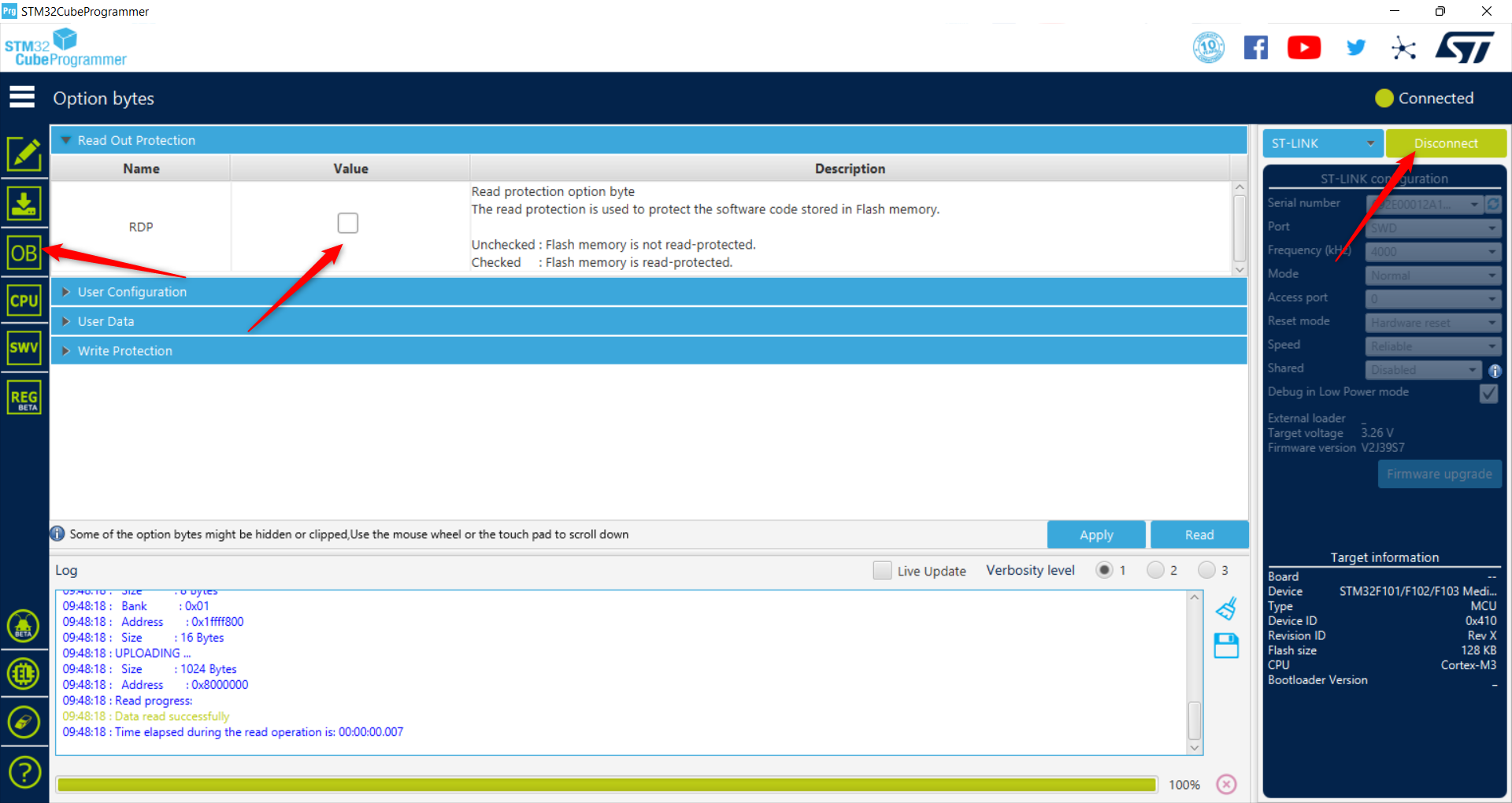
Figure 10.5: STM32CubeProgrammer. Enable RDP, Read protection
With read protection enabled, reading from flash is only possible when the microcontroller runs from main flash memory without any debug mode active. This can be reset, but then the flash is erased.
The STM32F103C8T6 flash is organized into 1 Kbyte pages. One bit of the WRP (Write protection) option bytes can set set to protect 4 pages of main flash memory in the STM32CubeProgrammer.
For more information on RDP and WRP, you can check [12].
10.2 STM32L5 and Nucleo-144
The following chapter focuses on the technical specifics and implementation details of TrustZone-M on a STM32L5 microcontroller. Chapter 10.3 accompanies this chapter and shows example firmware implementations on a STM32L5.
10.2.1 Hardware Overview
The cheapest development board with TrustZone-M support I could find was the NUCLEO-L552ZE-Q, which is powered by a STM32L552ZE microcontroller by STMicroelectronics. The hardware:
- Microcontroller: STM32L552ZET6QU
- Arm Cortex-M33 at 110 MHz with TrustZone and FPU
- Internal Flash Memory (512 KB)
- Internal SRAM1 (192 KB)
- Internal SRAM2 (64 KB)
The evaluation board provides:
- Different connectors like USB-Type C, SWD
- 3 LEDs
- 2 Push-Buttons
- On-Board ST-LINKv2-1 debugger and programmer
For the rest of this chapter I am going to refer to the evaluation board as Nucleo, and when I mean explicitly the microcontroller I use STM32L5.
Most of the values (memory regions,…) you will see in the next chapters are configurable by the user. I’ll use example values.
10.2.2 STM32 Product Life Cycle
The life cycle of a product, which contains a STM32L5 as a component, can be a hugely complex: After STM produced the STM32L5 there might be multiple vendors involved to assemble, initialize and provision the final product, before it is sold or delivered to the end user. The product might return to the vendor for Return Material Analysis or might be decommissioned. Different stages of the life cycle have different security requirements. For example, the original vendor might want to program the secure world of a device (e.g. to ensure it’s identity by storing secrets in secure world), but having the provisioning of nonsecure world outsourced to any other vendor.
10.2.2.1 Readout Protection (RDP)
The different security requirements of each development stage are reflected by Readout Protection (RDP) on STM32 devices. Different STM32 devices have different RDP levels with different features enabled or disabled per level. Transitioning between these levels is only possible in a predefined way. STM32L5 microcontrollers have the following RDP levels:
| RDP level | Description |
|---|---|
| 0 |
|
| 0.5 |
|
| 1 |
|
| 2 |
|
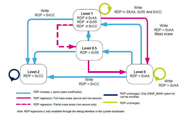
Figure 10.6: RDP transitions with TrustZone enabled (source: [13])
Figure 10.6 shows which transitions are possible in STM32L552x and on which transitions flash is erased. The example given above, where one vendor programs secure world and another one non-secure world, could be mapped by RDP transitions: Vendor 1 in RDP0 programs secure world and increases RDP to 0.5 and then ships the product to vendor 2, who programs non-secure world and increases to RDP 1 or 2. RDP 0.5 was introduced for these use cases and is only available, when TrustZone is enabled.
10.2.3 Option Bytes
Option Bytes are STM32L5s way to implement reset-enduring system configuration. These option bytes are automatically read back by the system on PoR. Using the STM32CubeProgrammer option bytes can be programmed for example via ST-Link. There are User Manuals and descriptions for STM32CubeProgrammer available on the product website.
To set the configuration bytes, the board must be plugged in and connected. To successfully connect to the board, the ST-Link drivers and the STM32CubeProgrammer (see chapter 10.3.1) need to be installed.
The option bytes are part of the flash information block. They can be reprogrammed through the flash interface registers at 0x5002 2000 - 0x5002 23FF (secure) and 0x4002 2000 - 0x4002 23FF (non-secure). There is a dedicated programming sequence you can find in [5, p. 190].
See chapter 10.3.2.1 for an example how option bytes are configured using the STM32CubeProgrammer.
10.2.4 Memory Map
In chapter 3.5 a high-level segmentation of the address space applicable to Arm6-M, Armv7-M and Armv8-M was introduced. The STM32L5 actually respects this Arm recommendations:
| region | from..to | Description |
|---|---|---|
| C-Bus access region | 0x0000 0000 .. 0x1FFF FFFF |
Access to flash, SRAM,… through C-Bus (with ICACHE) |
| SRAM 1 and SRAM2 | 0x2000 0000 .. 0x3FFF 0000 |
Access to SRAM1 and 2 through S-Bus |
| Peripherals | 0x4000 0000 .. 0x5FFF 0000 |
Access to Peripherals |
| FMC Bank 1 | 0x6000 0000 .. 0x7FFF 0000 |
Access to external memories managed through FSMC8 |
| FMC Bank 3 and OCTOSPI | 0x8000 0000 .. 0x9FFF 0000 |
Access to external memories managed through FSMC and OCTROSPI |
| Private Peripheral Bus, System region | 0xE000 0000 .. 0xFFFF FFFF |
Access to Cortex-M33 system control and debug. |
The memory map is divided into 512 MB sized regions, as Arm recommends for the system address map. The C-Bus access region is cached, where the first half of it is fixed (0x0000 0000-0x0FFF FFFF) and the other half can be used to remap external memories to be cached by ICACHE (0x1000 0000-0x1FFF FFFF). SRAM1 and SRAM 2 are accessible through the second 512 MB region (0x2000 0000 - 0x3FFF 0000). STM32L5x periperals are mapped to the region (0x4000 0000 - 0x5FFF 0000), wheras - in the Private Peripheral Bus region - Cortex-M33 peripherals and core registers are available (0xE000 0000 - 0xFFFF FFFF).
Some more details on the PPB can be found in chapter 3.5.
More on Arm Memory System:
10.2.4.1 STM32L5: IDAU and SAU
When TrustZone (TZEN=1 option byte) memory is either attributed as secure (S), non-secure (NS) or non-secure callable (NSC).The STM32L5 has one IDAU, which is used to further subdivide each of the regions from table 10.2 and attributes them to either NS and NSC areas, as you can see on figure 10.7.
![STM32L552xx IDAU memory mapping. [@rm0438 p. 87]](img/stm32-idau-memory-map.png)
Figure 10.7: STM32L552xx IDAU memory mapping. [5, p. 87]
More on Implementation Defined Attribution Unit:
STMicroelectronics decided not to predefine regions in IDAU as secure, but only split memory into NSC and NS. This leaves the choice to the developer to further decide which of the regions should be attributed secure (S).
As mentioned in the basics chapter on TrustZone-M (see chapter 4), the division of secure and non-secure worlds is - in contrast to TrustZone-A - memory map based. That might be a little bit difficult to wrap the head around, so let’s look at an example how flash can be split up (the values are from example 1, see chapter 10.3.2):
The STM32L5 has 512 KB Flash. Since we can address Flash bytewise, we need 0x0008 0000 addresses to address the whole Flash (512 * 1024). In figure 10.7 we see FLASH twice:
- 1:
0x0800 0000-0x0807 FFFF(NS) - 2:
0x0C00 0000-0x0C07 FFFF(NSC)
You can address whole Flash in both regions. When the system resets and TrustZone is enabled, whole memory (including 1 and 2) is secure by default. The next step for the developer is to configure SAU to downgrade up to 8 memory regions to either NSC or NS. In the IDAU and SAU security attribution logic, the highest of both attributes wins (see chapter 4.5). If a developer needs to define a NS region, she needs to downgrade a region in the SAU, which was also defined NS in IDAU (for the Flash example, that would be 1).
The example downgrades two regions in the SAU for Flash:
- Non-Secure
- IDAU attributes flash at
0x0800 0000to0x0807 FFFFas NS - The NS region in SAU is a subset of the NS region in IDAU, which is
0x0804 0000to0x0807 FFFF - The rest of it is attributed as S, because SAU is per-default S.
- IDAU attributes flash at
Because the other alias for Flash (region number 2) is attributed NSC in IDAU, you can’t downgrade it further than to NSC, so you need to choose region number 1 to define a NS region.
- Non-Secure Callable:
- IDAU attributes flash at
0x0C00 0000to0x0C07 FFFFas NSC. - NSC region in SAU is a subregion of the NSC region in IDAU, which is
0x0c03 E000to0x0c03 ffff. - The rest of it is attributed as S, because SAU is per-default S.
- IDAU attributes flash at
Remember: On PoR, when TrustZone is enabled, whole memory is secure by default in SAU. This is configurable in the ALLNS bit of the SAU_CTRL register. (see chapter 7.2). This leaves the regions, which are not downgraded in the SAU, as Secure.
This results in the final mapping of the whole 512 KB flash you can see on the far right on figure 10.7.

Figure 10.8: Flash Mapping Example 1
More on Security Attribution Unit:
In CMSIS the setup of SAU is done in the parition_<device>.h (see on GitHub). (see 7.2). The final Flash security attribution:
| Type | security attributes | from..to | description |
|---|---|---|---|
| Flash | NSC | 0x0C03 E000 - 0x0C03 FFFF | |
| Flash | NS | 0x0804 0000 - 0x0807 FFFF | |
| Flash | S | 0x0C00 0000 - 0x0C03 DFFF |
10.2.5 Global TrustZone Controller
The Global TrustZone Controller is a block on a STM32L5, which contains subblocks and components relevant for system security configuration. There are 3 subblocks, which are described later in this chapter.
IDAU and SAU is only one layer of security on a STM32L5. IDAU and SAU are only applicable for the Cortex-M33 as a master, but to protect Flash or SRAM from other masters, you need to configure the gates in front of the respective target. On figure 10.9 you can see how IDAU and SAU are only relevant for the Cortex-M33 core.

Figure 10.9: System Security in STM32L5
The importance of security on system level was already mentioned in chapter 4.7: On a system on a chip, the processing unit is only one actor in a complex system, the actors being interconnected on a bus system. In the STM32L5 there are 3 masters - two additional to the Cortex-M33 - which can issue transations on the bus and access peripherals, flash or SRAM. These are the DMA controller and the SDMMC controller. In the STM32L5 the security status of transactions issued by these masters are not filtered through IDAU and SAU configuration:
The SAU/IDAU settings are applicable to only the Cortex-M33. The other masters like DMA are not affected by those policies. [5]
To filter these transations either a security gate is added in front of the slaves or the slaves themselves are TrustZone-aware. When transactions from Cortex-M33 are initiated, this results in a transaction being filtered twice:
- IDAU / SAU
- by security gate or by TrustZone-aware peripheral itself
Other transactions, for example initiated by DMA master, are only filtered by the security gate in front of the slave.
The security gates in STM32L5 are configured through registes in the TrustZone security controller (TZSC). In STM32L5 the following peripherals have a security gate in front of them:
- SRAM
- peripherals
- External Memories
- External SRAM
For STM32L5 the following slaves are TrustZone aware, which means they don’t have a dedicated security gate in front of them. This also means, that they are not configured in the logical block of the GTZC, but in dedicated registers in the realm of the respective peripheral.
- Flash
- DMA
- Cortex-M33
- On-the-fly encryption/decryption (OTFDEC)
- Power Control (PWR), Secure clock and reset (RCC), Real time clock (RTC)
- Tamper and backup registers (TAMP)
- General-purpose I/Os (GPIO)
- Extended interrupts and event controller (EXTI)
- System configuration controller (SYSCFG)
The naming of the configuration registers follows their logical location: The SRAM for example has a block-based security gate in front. Since all security gates are part of the GTZC, the register to configure the SRAM security gate is named GTZC_MPCBB_* (it is a block-based memory protection gate). The flash on the other side is itself TrustZone-aware, so it’s security configuration registers are prefixed with FLASH_*.
| Component | Security configuration register names |
|---|---|
| SAU | SAU_* - Part of Cortex-M33 |
| SRAM | GTZC_MPCBB_* (non-aware, configured in TZSC, which is part of GTZC) |
| Peripherals (not aware) | GTZC_TZSC_* |
| Peripherals(TZ aware) | Configured in eachs space, eg for RCC: RCC_*. |
| Flash | FLASH_* (TrustZone-aware) |
STM32L5 implements a Global TrustZone controller (GTZC), with the following sub-blocks:
- TrustZone security controller (TZSC): Chapter 10.2.5.1
- TrustZone illegal access controller (TZIC): Chapter 10.2.5.2
- SRAM security configuration (block-based security gate, MPCBB): 10.2.5.3
Since Flash itself is TrustZone aware it does not logically belong to the GTZC. The security configurations for Flash are highly relevant for overall system security, so it does make sense to describe them in the current chapter:
- Flash security configuration (watermark-based security gate): Chapter 10.2.5.4
More on System Security Components:
- Chapter 4.7.1: System Security Controller
- Chapter 4.7.2: Security wrapper
- Chapter 4.7.3: Block-based Gate
- Chapter 4.7.4: Watermark-based Gate
- Chapter 4.7.5: Select-based Gate
- Chapter 4.7.6: Lite-IDAU
- Chapter 10.2.5.2: STM32L5: TrustZone Illegal Access Controller (TZIC)
- Chapter 10.3.2.2: Example STM32L5: GTZC Configuration (Example 1)
More on System Security Design:
TrustZone security controller (TZSC)
The TZSC is the component on STM32L5 which configures the secure and privilege state of slave and masters on the bus, e.g. whether the slave is only available in secure and/or privileged state. This is done by configuring the different gates,- which are in front of TrustZone unaware peripherals (like the watermark based gate) but also the security wrappers, which are in front of masters to correctly attribute transactions issued by non-TrustZone aware masters. (see chapter 4.7.2).
You can find more details on the TZSC in chapter 10.2.5.1.
TrustZone illegal access controller (TZIC)
The STM25L5 has 109 interrupts configured, plus the ARMv8-M default execeptions. One of these 109 interrupts is the GTZC interrupt at position 8. This interrupt is raised by TZIC, if an illegal access event has been reported to it by any gate. The TZIC concentrates all illegal access events. To determine which gate caused the illegal access event, developers can check registers in TZIC in the GTZC IRQ.
You can find more details on the TZIC in chapter 10.2.5.2.
10.2.5.1 TrustZone Security Controller (TZSC)
More on Arm Privilege Levels:
The sub-block TrustZone Security Controller (TZSC) defines the security level of slave and master peripherals to secure or non-secure state but also to privileged or unprivileged. These settings are done in the following registers:
GTZC_TZSC_SECCFGRx: Holds 1 bit per peripheral, which represents its security state (Secure or Non-Secure access). Reset value:0x0000 0000, which is non-secure.GTZC_TZSC_PRIVCFGRx: Holds 1 bit per peripheral, which represents its privilege state (privilege or non-privileged access). Reset value:0x0000 0000, which is non-privileged.
Where x ={1,2}
10.2.5.1.1 STM32CubeL5 HAL for TZSC
If you use the STM32CubeMX code generator to ramp up you project, you will find the necessary code to initialize GTZC in the function MX_GTZC_Init(void) in main.c. For TZSC it uses - depending on your configuration- the following HAL API functions:
HAL_GTZC_TZSC_ConfigPeriphAttributes(),HAL_GTZC_TZSC_GetConfigPeriphAttributes()to configure the peripherals you configured as secure and or privileged. This HAL functions set up the registersGTZC_TZSC_SECCFGRxandGTZC_TZSC_PRIVCFGRxaccordingly.HAL_GTZC_TZSC_Lock()/HAL_GTZC_TZSC_GetLock()to lock TZSC against modifications (until complete reset of TZSC). This HAL functions set up the GTZC_TZSC control register (GTZC_TZSC_CR) accordingly.
Examples:
- GTZC initialization in Example 1: Chapter 10.3.2.2
10.2.5.2 TrustZone Illegal Access Controller (TZIC)
See chapter 10.3.2.2 and chapter 10.3.2.4 for an example implementation, which uses STM32 HAL and the implemented GTZC TZIC callback to check an illegal access event.
TrustZone-aware peripherals and security gates report illegal access events to the TZIC. The TZIC then generates an interrupt (GTZC_IRQn) towards the NVIC. Illegal access events reported to TZIC can be:
- illegal non-secure access: a non-secure transaction trying to access a secure component
- illegal secure access:
- a secure transaction trying to access non-secure SRAM, as defined by the block-based firewall.
- a secure transaction trying to access non-secure watermark-based firewall protected external memories
The TZIC generates one interrupt for different events. To find out which event triggered the interrupt, TZIC provides different registers to filter. TZIC also provides means to mask events and thus disable generation of GTZC_IRQn per event.
GTZC_TZIC_IERn: The GTZC_TZIC Interrupt Enable Register is used to mask individual events generating GTZC_IRQs towards the NVIC. Default: All events are masked.GTZC_TZIC_SRn: The GTZC_TZIC Status Register is used to show which source created the illegal access. There is a flag for each peripheral.GTZC_TZIC_FCRn: The GTZC_TZIC Clear Register is used to clear the flags set in GTZC_TZIC_SRn.
Where n = {1,2,3}.
More on Arm Exception System:
- Chapter 3.6.2: Arm Architecture:NVIC
- Chapter 3.6.3: Arm Architecture: Masking
- Chapter 6.3: Exception Entry and Return
- Chapter 10.2.5.2: STM32L5: TrustZone Illegal Access Controller (TZIC)
- Chapter 3.4: Arm Architecture: Execution Modes and Privilege Levels
- Chapter 3.6: Arm Architecture:Exceptions, Interrupts, Faults
- Chapter 7.5: Secure and non-secure exceptions
SAU and IDAU are located in the core block and thus don’t report illegal events to TZIC. Violations of the SAU/IDAU security policy are reported directly to the core using a SecureFault exception. Sidenote: Armv8-M cores without the main extension (base only), don’t have a SecureFault and use a HardFault exception. For more details see the next level box above.
10.2.5.2.1 STM32 HAL for TZIC
HAL_GTZC_TZIC_DisableIT()/HAL_GTZC_TZIC_EnableIT()to mask / unmask the reporting of illegal access event for peripherals, which are configured to report their illegal access events to the TZIC.HAL_GTZC_TZIC_GetFlag()/HAL_GTZC_TZIC_ClearFlag()to control flags inGTZC_TZIC_SRnandGTZC_TZIC_FCRn.There is a default interrupt handler for GTZC_IRQn implemented, which is named
HAL_GTZC_IRQHandler(). Developers can can add own code usingHAL_GTZC_TZIC_Callback()
Examples:
- TZIC configuration in Example 1: Chapter 10.3.2.2
10.2.5.3 SRAM
The STM32L552x has up to 256 Kbytes of internal SRAM:
- 192 KBytes of SRAM1
- 64 Kbytes of SRAM2
There are different security options available on STM32L552x:
- When TrustZone is enabled, SRAM2 can be write protected on a 1 KByte granularity.
- When Read Out Protection is enabled (see 10.2.2.1), SRAM is also protected.
- When TrustZone is enabled, SRAM is attributed secure by default and can be reattributed to non-secure on a 256 byte sized granularity through the block-based memory protection controller.
Write Protection is configured in SYSCFG (System Configuration Controller) block. The respective registers are:
SYSCFG_SWPRSYSCFG_SWPR2
If TrustZone is not enabled, there is no access restriction.
SRAM is not TrustZone-aware and thus has a block-based gate in front of it. Actually, there are two MPCBB (block-based memory protection controller) blocks: MPCBB1 is in front of SRAM1 and MPCBB2 in front of SRAM2. According to the logic determined in table 10.4 the respective configuration registers are located in GTZC and named accordingly:
GTZC_MPCBBx_VCTRy
Where x is 1 or 2 (for MPCBB1 and MPCBB2) and y is a register of 32 bit. There registers are reset to 0xFFFF FFFF, so whole SRAM is secure (when TrustZone is enabled). Security configuration of MPCBB can also be locked using the registers GTZC_MPCBBx_LCKVTRy.
More on SRAM Protections:
10.2.5.3.1 STM32 HAL for SRAM Security Configuration
- The HAL provides multiple functions to configure SRAM MPCBB1 and 2:
HAL_GTZC_MPCBB_ConfigMem()andHAL_GTZC_MPCBB_ConfigMemAttributes() - To configure the lock or get the lock status:
HAL_GTZC_MPCBB_Lock()andHAL_GTZC_MPCBB_GetLock().
10.2.5.4 Flash
The internal Flash can be divided into main block and an information block. The information block is used to store configuration, ST propierary code and OTP data. Only parts of the information can be modified by the user, other parts are reserved for STM. The information block is also used to store the option bytes. See chapter 10.3.2.1 for an example option byte configuration.
The main block can be run into 1 or 2 banks (dual bank mode, DBANK=1 option byte). Dual bank mode offers the possibility to read on one bank, while executing on the other (Read-while-write (RWW)). The page size differ in each mode:
- DBANK=0: page size is 4 KByte
- DBANK=1: page size is 2 KByte
STM32L552x brings multiple protection mechanisms for flash memory:
- Write Protection (WRP):
- DBANK=0: 4 areas, page granularity
- DBANK=1: 2 areas per bank, page granularity
- Readout Protection (RDP)
When TrustZone is enabled, Flash can be further protected by:
Secure watermark-based area (SECWM): Protection against non-secure read and write access. This is the state Flash is in per-default, when TrustZone is enabled.
- DBANK=0: 2 areas, page granularity
- DBANK=1: 1 per bank, page granularity
Secure block-based area (SECBB): Flash pages can be programmed on-the-fly as “secure,” when they are marked as nonsecure in SECWM.
Secure hide protection (HDP): Parts of SECWM regions can be further protected by hiding them until the next reset. When HDP protections for a region is enabled, read, write and fetch is denied for that region.
- DBANK=0: 2 areas, page granularity
- DBANK=1: 1 area per bank, page granularity
More on Flash Protections:
Write Protection (WRP) is configured in the option bytes FLASH_WRP1AR, FLASH_WRP1BR, FLASH_WRP2AR, FLASH_WRP2BR. The areas protected against write operations are configured relative to the flash base address. Details can be found in [5, p. 201].
Depending on the RDP level (0, 1 or 2) different protections are applied to flash. The default level is 0, which has no protections. See 10.2.2.1 for details on flash protections in each level. Additional details are available in [5, p. 203].
When TrustZone is active flash memory can further be protected against non-secure read and write access. There are two secure areas the developer can define in the option bytes. The areas are defined by a start and end page offset. This Secure watermark-based area (SECWM) is configured in the option bytes register FLASH_SECWMnR1 where n = {1,2}. These 2 registers contain different option bytes, where the start and end page offsets can be set:
SECWMn_PSTARTSECWMn_PEND
See chapter 10.3.2.1 for an example on SECWM_* configuration.
Watermarked areas can further be protected by Hide Protection (HDP). If a watermarked area in flash is further protected by hide protections, read, write and fetch on this area is denied until the next device reset. HDP is configured in FLASH_SECWMnR2 where n = {1,2}. These two registers contain two option bytes:
HDPnENHDPn_PEND
If HDPnEN = 1 and SECWMn_PSTRT <= HDPn_PEND <= SECWMn_PEND the area between SECWMn_PSTRT and HDPn_PEND is hide protected.
Additionally to the configuration in FLASH_SECWMnR2, the bit HDPn_ACCDIS in flash register FLASH_SECHDPCR must be enabled, to deny access to the respective HDP area. This register is not loaded from flash and used to enable HDP by the developer.

Figure 10.10: Watermark and Hide Protected Area in STM32L5
10.2.5.4.1 STM32 HAL for Flash Security Configuration
STM32 HAL provides functions to program the protection mechanisms through HAL.
HAL_FLASHEx_OBProgram (FLASH_OBProgramInitTypeDef * pOBInit)can be used to program option bytes.FLASH_OBProgramInitTypeDefis a struct which holds fields for all the fields to configure all protections mentioned in the chapter above, including the watermark and hide protected areas.HAL_FLASHEx_EnableSecHideProtection()can be used to configureHDPn_ACCDISinFLASH_SECHDPCR.
9 Flexible static memory controller
10.3 Examples: STM32 Nucleo-144
The previous chapters laid the foundation by providing an overview on basic topics from implementation using C language to TrustZone-M. Then chapter 10.2 provided an overview on the most important features of a STM32L5 microcontroller. All these basic chapters are used in the following examples and should make understanding the examples much easier. The goal of this chapter is to develop both secure and non-secure world example firmwares.
Currently the following examples are implemented:
The following examples are implemented on the hardware described in chapter 10.2.1.
Please note: Neither the code nor the option byte configuration is suitable for production use. Don’t copy your code from the internet in real world projects!
10.3.1 Tools and Hardware Configuration
There are some prerequisites to successfully reproduce the example:
The following links and softwares are used through this chapter:
STM32CubeIDE is an Integrated Development Environment. Based on open-source solutions like Eclipse or the GNU C/C++ toolchain, this IDE includes compilation reporting features and advanced debug features. It also integrate additional features present in other tools from the ecosystem, such as the HW and SW initilialization and code generation from STM32CubeMX.[14]
STM32CubeIDE is also TrustZone aware.
STM32CubeProgrammer * ST-Link drivers.
STM32CubeProgrammer provides an easy-to-use and efficient environment for reading, writing and verifying device memory through both the debug interface (JTAG and SWD) and the bootloader interface (UART and USB).[14]
STM32CubeMX. STM32Cube initialization code generator.
STM32CubeMX is a graphical tool used to configure any STM32 device. This easy-to-use graphical user interface generates the initialization C-code for Cortex-M cores and generates the Linux Device Tree for Cortex-A cores.[14]
Personally I am running all these tools in a Windows 10 VM and I pass the STM32Link device from the Host through to the VM. That setup until know seems to work pretty stable.
I recommend the following steps:
- Install all Tools listed above.
- Do the initial Hardware setup for the respective project.
- Check out the example code and import it to STM32CubeIDE.
- Compile and run the example without modifications
10.3.1.1 STM32CubeIDE Setup
STM provides a pretty good guide on how to work with TrustZone enabled projects for STM32L5 cores with their STM32CubeIDE in AN5394: Getting started with projects based on the STM32L5 Series in STM32CubeIDE. This Application Note includes a guide on how to import an existing projects, so I won’t replicate that content here.
You can use the “Import” function of STM32CubeIDE to work on the examples, after you cloned them from the repository.
10.3.2 Secure Random Number Generator (Example 1)
You can find the source code for this example on GitHub.
Example 1 implements secure and non-secure firmware for the Nucleo-144 with the following features:
Secure world: There is a function callable from NS, which generates a random number using the hardware random number generator. The random number is returned to NS world.
Secure world: There is a function callable from NS, which takes a random number and writes it to UART.
Non-secure world:
main()generates a random number and writes it to UART. The user can decide upon pressing a physical button whether the random number is generated using the secure world function (not pressed) or by trying to access the hardware random generator from non-secure world directly. (pressed). Writing to UART is always done using the secure world.Illegal accesses to the RNG is visualized by blinking the red LED. The system also prints a security violation message on UART and then resets.
The system security settings are:
- The random number generator security state is secure.
- The UART (LPUART) security state is is secure.
- The Button (PC13) security state is non-secure.
The idea is, that we as an user can trigger a security violation by pressing the button: When the user presses the button, main() in non-secure world will try to generate the random number directly and thus will trigger a security violation, because the RNG is mapped to secure world only.
After running the firmware on the Nucleo and connecting to the board over UART, you are going to see random numbers appearing on the screen. Then, if you press the blue button, security violation will occur and the system will reset:
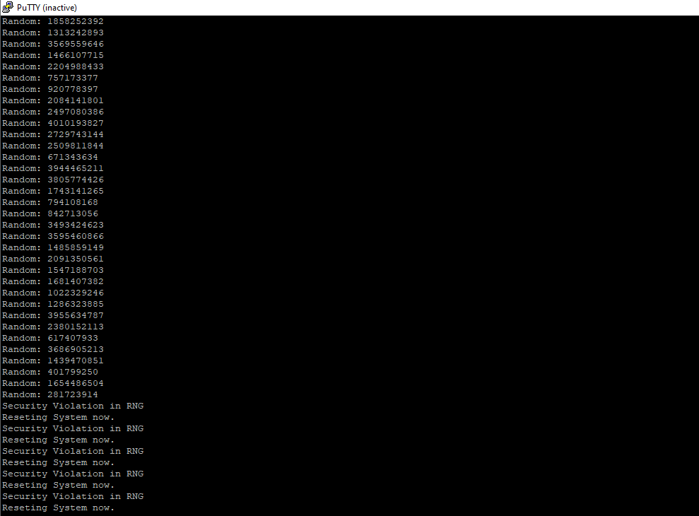
Figure 10.11: Example 1 running. The last few messages show a security violation, when the button was pressed and the system resetted itself.
STM32 uses a ported version of CMSIS for the projects created in STM32CubeProgrammer. To get an overview on CMSIS in general, follow the links in the NextLevel box below.
10.3.2.1 Option Bytes Configuration
As describes in 10.2.3 in detail, option bytes are used to do reset-enduring system configuration. These option bytes are automatically read back by the system on PoR.
The following option bytes settings are used in the example implemented in this chapter. For other projects you might want to adjust the settings.
To enlarge the following pictures, open them by right-click and then “open in New Tab” *
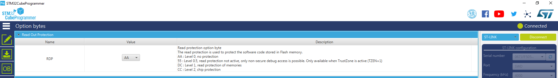
Read-out protection. You can find technical details on the Read-out protections (RDP) in chapter 10.2.2.
For this example, RDP level is set to AA, which is no protection: Level 0.
More on Lifecycle Configurations:
- Chapter 10.2.2.1: STM32 Product Life Cycle
STM32CubeProg: RDP Settings
TZEN, SECBOOTADD0, NSBOOTADD0. TrustZone and the Boot addresses are set up in the configuration bytes. Also the watermark protected areas are set up here. Details on watermarked areas are described in chapter 10.2.5.4.
- TrustZone is enabled via TZEN=1
- Hide protected areas are not enabled.
More on Flash Protections:
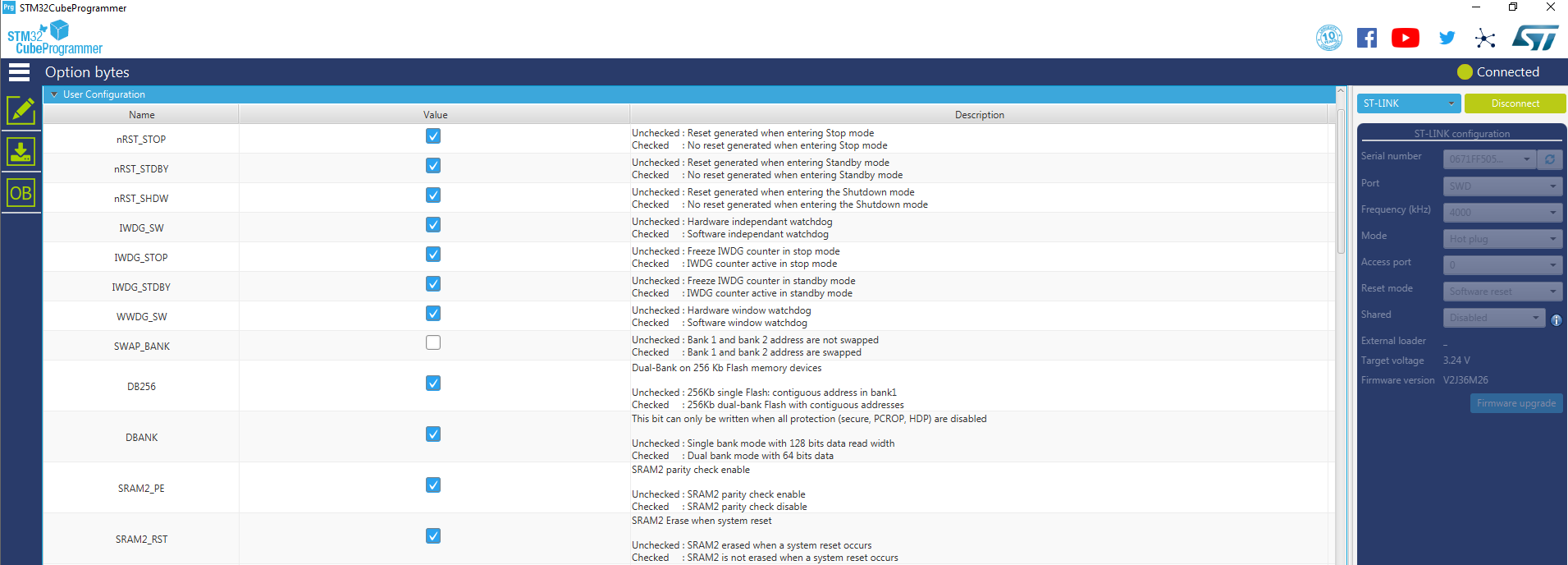
STM32CubeProg: User Configuration
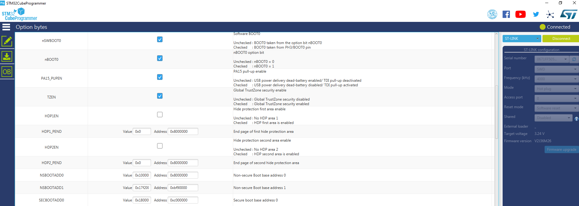
STM32CubeProg: User Configuration
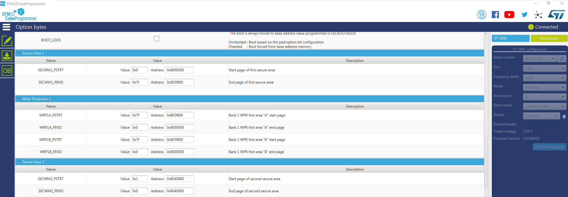
STM32CubeProg: User Configuration
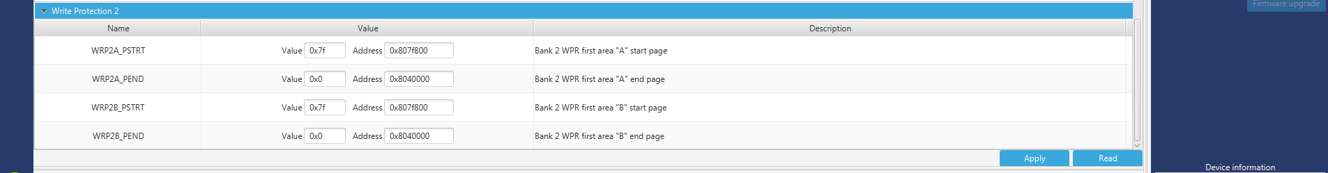
STM32CubeProg: User Configuration
10.3.2.2 GTZC Configuration
In this example project was set up by the STM32CubeMX. Thus GTZC is also set up by the initialization code generated by STM32CubeMX. Follow the links in the NextLevel box for details on how GTZC and its sub-components are configured using the STM32 HAL.
See 10.3.3.1.1 in the appendix of this chapter for the STM32CubeMX setup of this project.
More on STM32L5: GTZC and subcomponents:
- Chapter 10.2.5.1: TrustZone Security Controller (TZSC)
- Chapter 10.2.5.1.1: STM32CubeL5 HAL for TZSC
- Chapter 10.2.5.2: STM32L5: TrustZone Illegal Access Controller (TZIC)
- Chapter 10.2.5.2.1: STM32CubeL5 HAL for TZIC
- Chapter 10.2.5.3: STM32L5: SRAM
In this example STM32CubeMX generated the following GTZC initialization code MX_GTZC_Init() according to chapter 10.3.3.1.1 in the appendix. As we can see
- the peripherals
RNGandLPUART1are mapped to secure world usingHAL_GTZC_TZSC_ConfigPeriphAttributes() - the block-based memory protection controller is set up (mapping SRAM to secure / non-secure worlds) using the HAL function
HAL_GTZC_MPCBB_ConfigMem(). - TZIC interrupts for RNG and Flash security events are enabled using the HAL function
HAL_GTZC_TZIC_EnableIT().
You can find an explanation on the HAL API in the respective chapters. See the links in the box above.
MX_GTZC_Init(void) on GitHub.
static void MX_GTZC_Init(void)
{
  MPCBB_ConfigTypeDef MPCBB1_NonSecureArea_Desc = {0};
  MPCBB_ConfigTypeDef MPCBB2_NonSecureArea_Desc = {0};

  if (HAL_GTZC_TZSC_ConfigPeriphAttributes(GTZC_PERIPH_LPUART1, GTZC_TZSC_PERIPH_SEC|GTZC_TZSC_PERIPH_NPRIV) != HAL_OK)
  {
    Error_Handler();
  }

  if (HAL_GTZC_TZSC_ConfigPeriphAttributes(GTZC_PERIPH_VREFBUF, GTZC_TZSC_PERIPH_SEC|GTZC_TZSC_PERIPH_NPRIV) != HAL_OK)
  {
    Error_Handler();
  }

  if (HAL_GTZC_TZSC_ConfigPeriphAttributes(GTZC_PERIPH_RNG, GTZC_TZSC_PERIPH_SEC|GTZC_TZSC_PERIPH_NPRIV) != HAL_OK)
  {
    Error_Handler();
  }

  MPCBB1_NonSecureArea_Desc.SecureRWIllegalMode = GTZC_MPCBB_SRWILADIS_ENABLE;
  MPCBB1_NonSecureArea_Desc.InvertSecureState = GTZC_MPCBB_INVSECSTATE_NOT_INVERTED;
  [...]
  MPCBB1_NonSecureArea_Desc.AttributeConfig.MPCBB_LockConfig_array[0] =   0x00000000;

  if (HAL_GTZC_MPCBB_ConfigMem(SRAM1_BASE, &MPCBB1_NonSecureArea_Desc) != HAL_OK)
  {
    Error_Handler();
  }

  MPCBB2_NonSecureArea_Desc.SecureRWIllegalMode = GTZC_MPCBB_SRWILADIS_ENABLE;
  [...]
  MPCBB2_NonSecureArea_Desc.AttributeConfig.MPCBB_LockConfig_array[0] =   0x00000000;
  if (HAL_GTZC_MPCBB_ConfigMem(SRAM2_BASE, &MPCBB2_NonSecureArea_Desc) != HAL_OK)
  {
    Error_Handler();
  }
  if (HAL_GTZC_TZIC_EnableIT(GTZC_PERIPH_RNG) != HAL_OK)
  {
    Error_Handler();
  }
  if (HAL_GTZC_TZIC_EnableIT(GTZC_PERIPH_FLASH) != HAL_OK)
  {
    Error_Handler();
  }

}
10.3.2.3 Peripheral Configuration
STM32CubeMX also does automatically add code for settings up LPUART, RNG and the GPIOs for the LEDs. Overall the following functions will be generated automatically:
static void MX_GPIO_Init(void);
static void MX_GTZC_Init(void);
static void MX_RTC_Init(void);
static void MX_LPUART1_UART_Init(void);
static void MX_RNG_Init(void);
Additionally file scope handles to the peripherals will be added to your main.c, which you can use to access the peripherals:
UART_HandleTypeDef hlpuart1;
RNG_HandleTypeDef hrng;
10.3.2.4 Secure World Implementation
Check chapter 10.3.2 for a list of features we want to implement.
Please note: This code is not production ready and only for demonstration purposes. Don’t copy and paste code from the internet :)
Two secure functions were implemented and declared as entry functions. The first one is to generate and return a random number in secure world (CMSE_NS_ENTRY uint32_t SECURE_GenerateRandom()) and return the number to the non-secure world. The handle (hrng) was configured and set up by the STM32CubeMX code generator.
The second one secure world entry function takes a random number and transmits it over the LPUART interface. (CMSE_NS_ENTRY void SECURE_TransmitRandomUart(uint32_t random32bit))
In the previous chapters on the basic topics we already discussed how secure functions are implemented and how they return values. Please check the Next Level box above for details.
More on Secure function calls:
main.c:
- uint32_t SECURE_GenerateRandom() on GitHub
- void SECURE_TransmitRandomUart() on GitHub
CMSE_NS_ENTRY uint32_t SECURE_GenerateRandom(){
    uint32_t random32bit;
    HAL_StatusTypeDef status = HAL_ERROR;
    status = HAL_RNG_GenerateRandomNumber(&hrng, &random32bit);
    while (status == HAL_ERROR){}
    return random32bit;
}

CMSE_NS_ENTRY void SECURE_TransmitRandomUart(uint32_t random32bit){
    char buff[50];
    sprintf(buff, "Random: %lu\r\n", random32bit);
     HAL_StatusTypeDef status = HAL_UART_Transmit(&hlpuart1, (uint8_t*) buff, strlen(buff), 1000);
     if (status != HAL_OK){
         Error_Handler();
     }
}
To notify the user about illegal accesses to the RNG by blinking the LED and resetting the system, we need the STM32 GTZC HAL callback function named HAL_GTZC_TZIC_Callback. The GTZC HAL implements an interrupt handler for the GTZC_IRQ, which in turn calls the callback when the interrupt is triggered. The peripheral which caused the illegal access is passed to the callback as parameter periph.
main.c:
- void HAL_GTZC_TZIC_Callback() on GitHub
void HAL_GTZC_TZIC_Callback(uint32_t periph){
        if(periph == GTZC_PERIPH_RNG){
            HAL_GPIO_WritePin(LED_RED_GPIO_Port, LED_RED_Pin, 1);
            TransmitCharPUart("Security Violation in RNG\r\nReseting System now.\r\n");
            HAL_NVIC_SystemReset();
        }
}

void TransmitCharPUart(char* text){
     HAL_StatusTypeDef status = HAL_UART_Transmit(&hlpuart1, (uint8_t*) text, strlen(text), 1000);
     if (status != HAL_OK){
         Error_Handler();
     }
}
10.3.2.5 Non-Secure World Implementation
Check chapter 10.3.2 for a list of features we want to implement.
The function NONSECURE_GenerateRandom() accesses the RNG directly and not by calling the secure world function implemented above. (see chapter 10.3.2.5.1)
In main() we generate the random number depended on the state (pressed / not pressed) of the button on the Nucleo-144. When the button is pressed non-secure world firmware tries to generate a random number directly (by calling NONSECURE_GenerateRandom). In non-pressed state SECURE_GenerateRandom() is used. In the first case an illegal access event is raised and the GTZC_IRQn is issued from TZIC. See chapter 10.3.2.2.
main.c:
- uint32_t NONSECURE_GenerateRandom() on GitHub
uint32_t NONSECURE_GenerateRandom(){
    MX_RNG_Init();
    uint32_t random32bit;
    HAL_StatusTypeDef status = HAL_ERROR;
    status = HAL_RNG_GenerateRandomNumber(&hrng, &random32bit);
    while (status == HAL_ERROR){}
    return random32bit;
 }

int main(void)
{
  HAL_Init();

  MX_GPIO_Init();
  MX_ADC1_Init();
  MX_RTC_Init();

  while (1)
  {
      uint32_t random32bit;
      GPIO_PinState button = HAL_GPIO_ReadPin(GPIOC, GPIO_PIN_13);
      if(button)
          random32bit = NONSECURE_GenerateRandom();
      else
          random32bit = SECURE_GenerateRandom();
      HAL_Delay(1000);
      SECURE_TransmitRandomUart(random32bit);
  }
}
10.3.2.5.1 RNG in Non-Secure world
To raise an illegal access from non-secure world by accessing the RNG without having it mapped to non-secure world, we copy the RNG initialization code from secure world (especially MX_RNG_Init) into the non-secure world project, but don’t update the security configuration of the RNG.
To have all needed definitions available in main.c, we first need to uncomment
#define HAL_RNG_MODULE_ENABLEDin stm32l5xx_hal_conf.h (on Github).
Then we copy the following code into main.c:
RNG_HandleTypeDef hrng;

static void MX_RNG_Init(void)
{

  hrng.Instance = RNG;
  hrng.Init.ClockErrorDetection = RNG_CED_ENABLE;
  if (HAL_RNG_Init(&hrng) != HAL_OK)
  {
    Error_Handler();
  }

}
10.3.3 Appendix
10.3.3.1 Example 1
10.3.3.1.1 Initial Project Configuration
This chapter is for reference. The example on GitHub contains an ioc file, which has the following configuration already applied. If you want to create your own ioc for the project, follow through the step of this chapter.
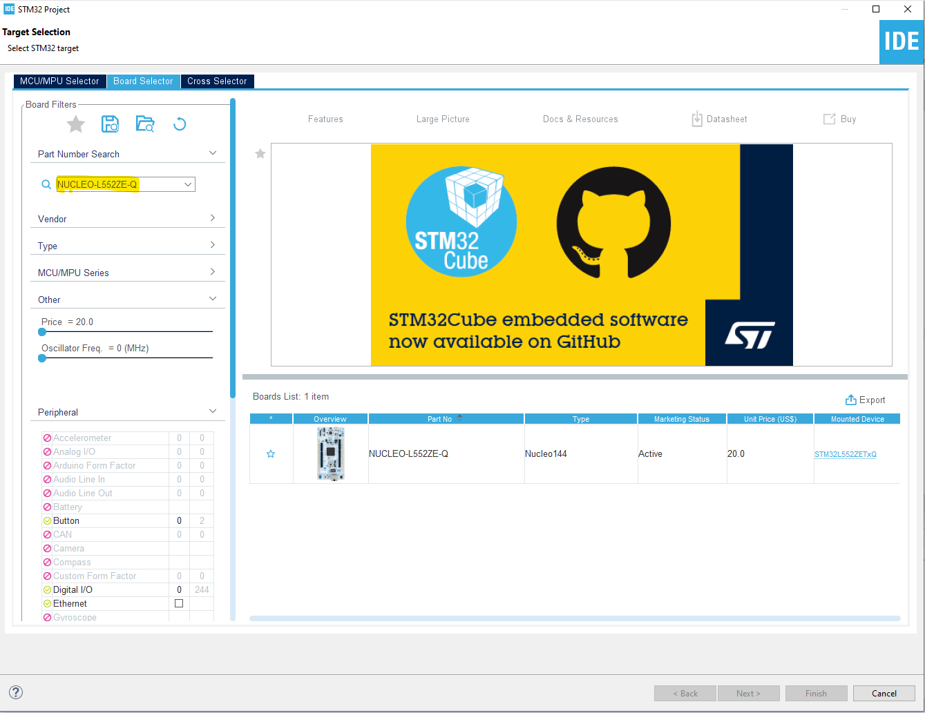
Figure 10.12: Example Project Configuration: Project Setup
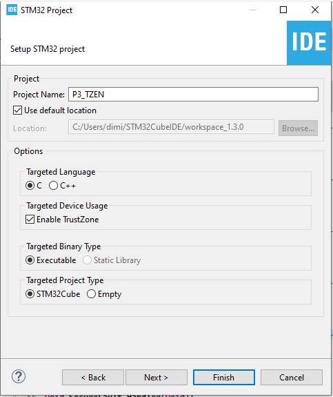
Figure 10.13: Example Project Configuration: Project Setup
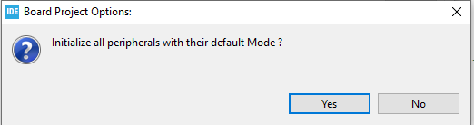
Figure 10.14: Example Project Configuration: Project Setup
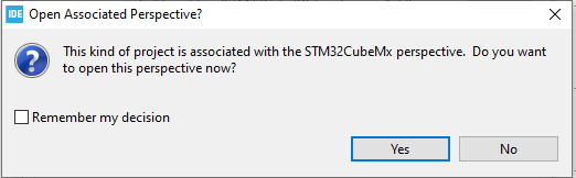
Figure 10.15: Example Project Configuration: Project Setup
10.3.3.1.1.1 GTZC Configuration
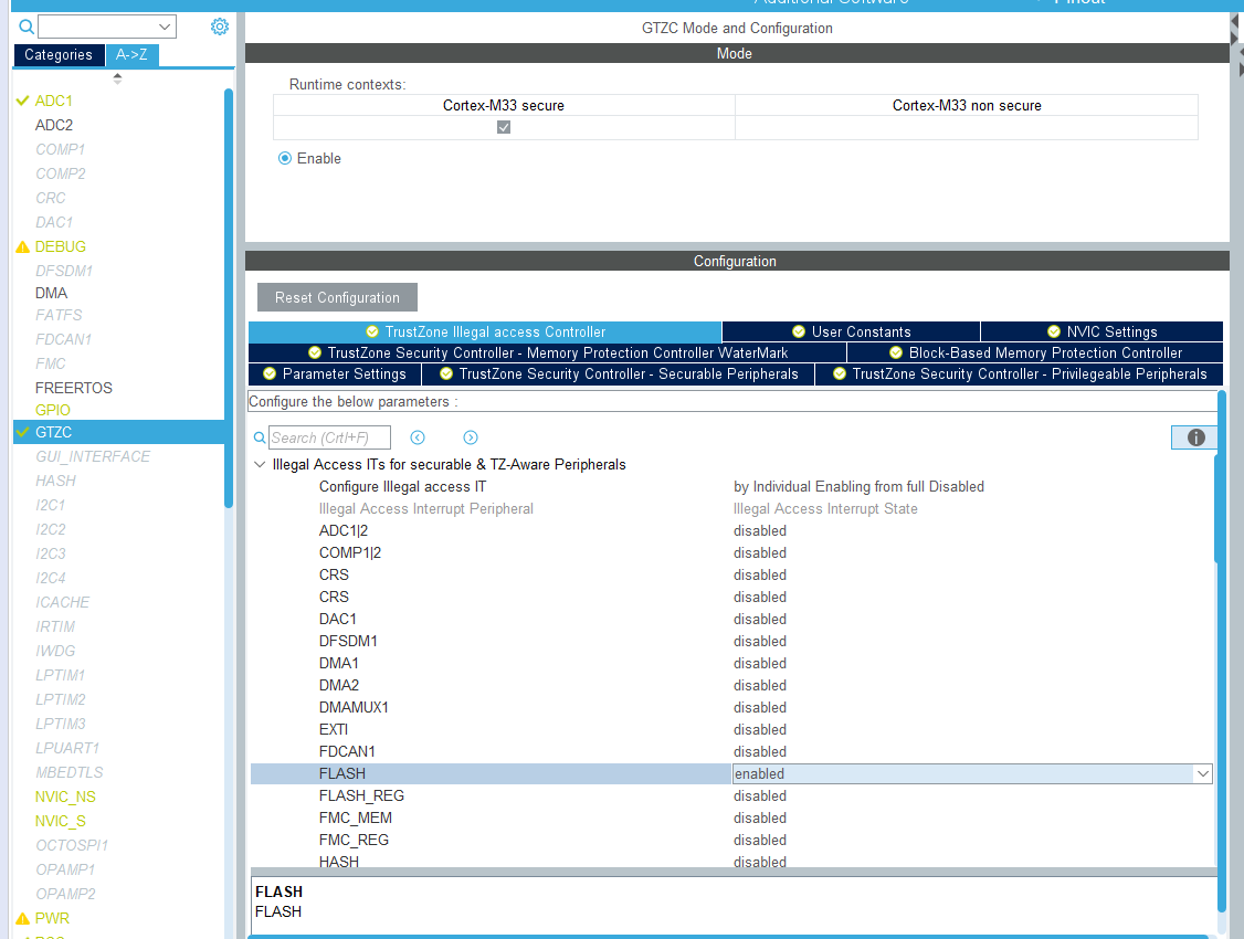
Figure 10.16: Example Project Configuration: GTZC Configuration
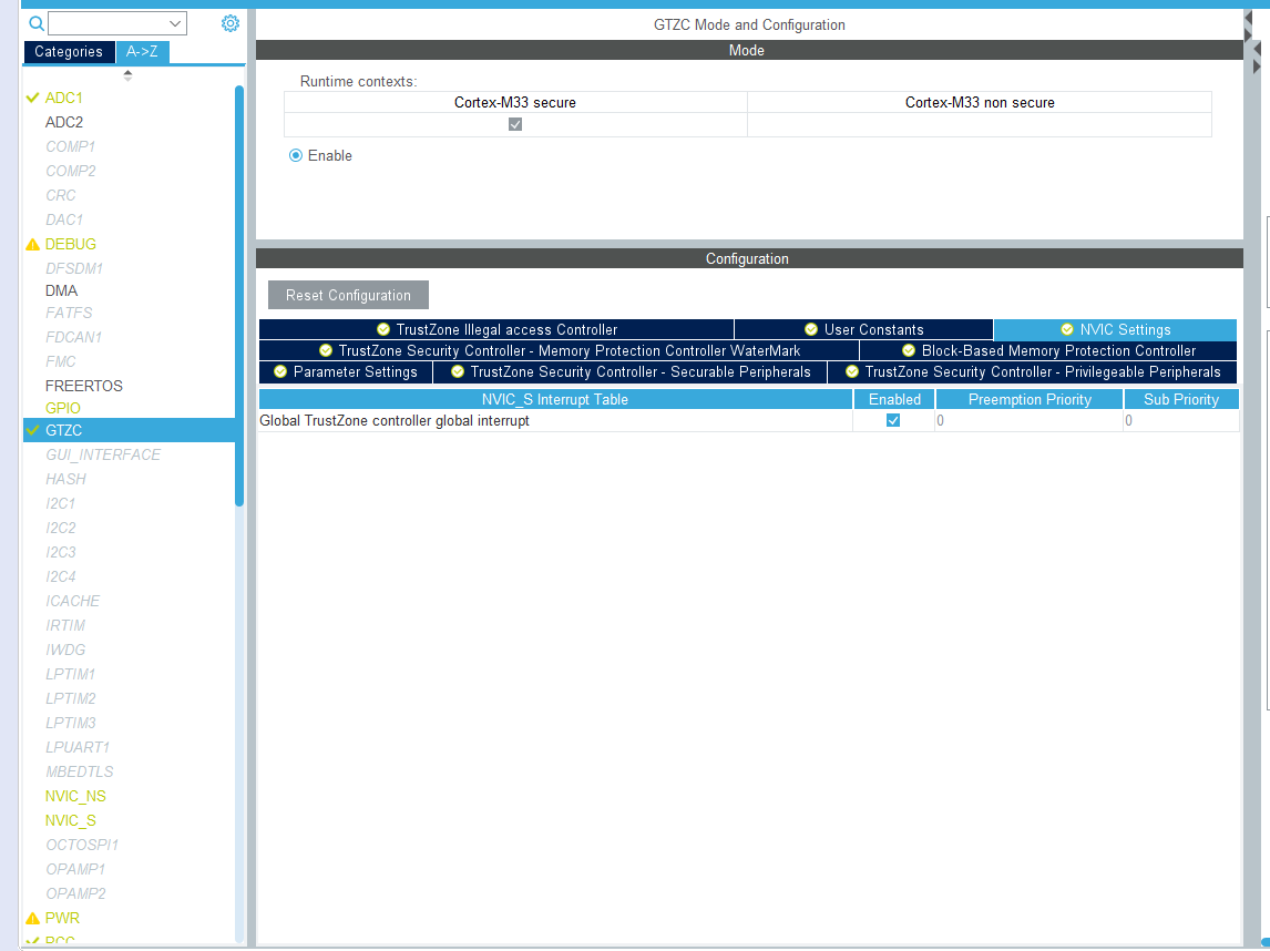
Figure 10.17: Example Project Configuration: GTZC Configuration
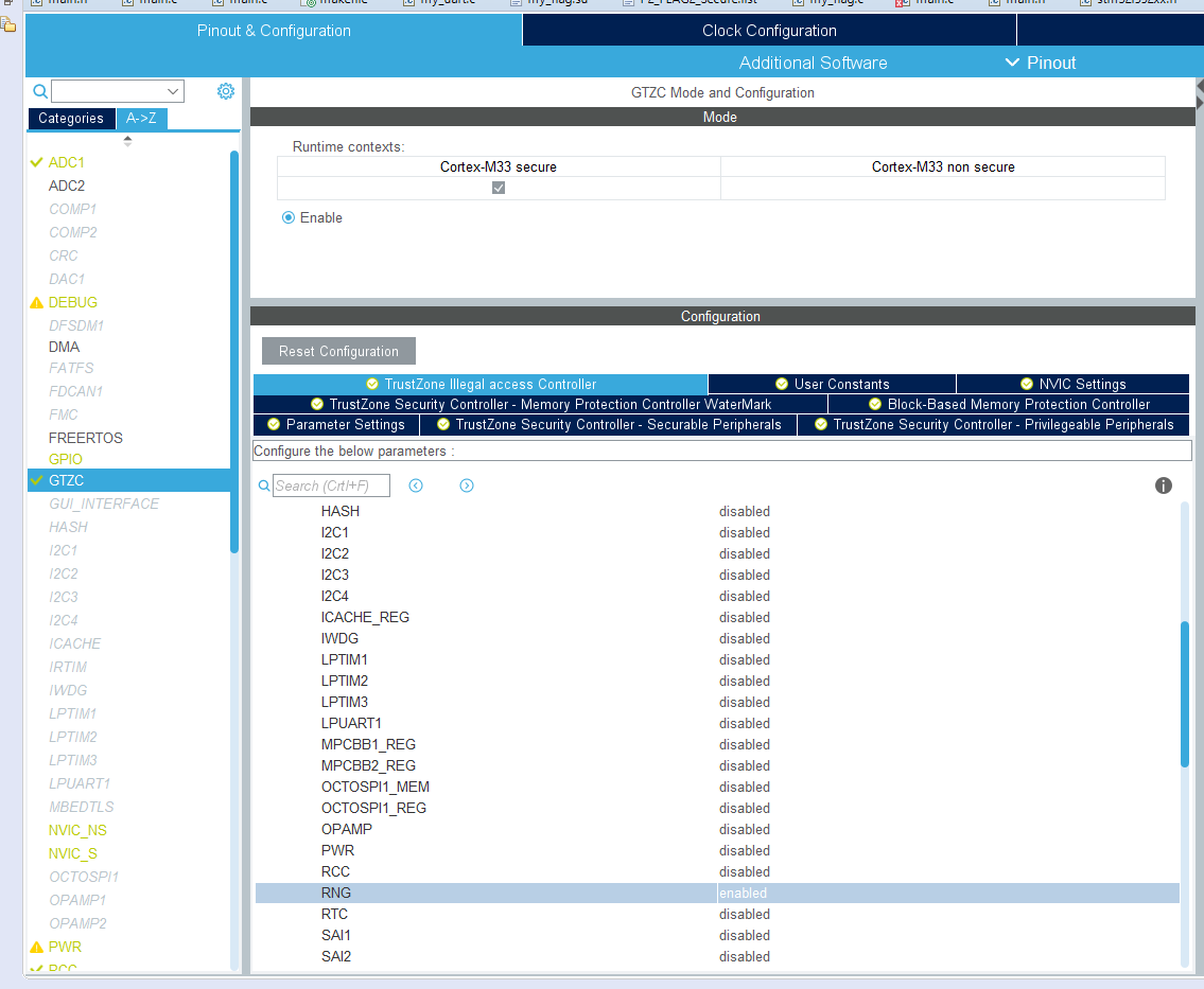
Figure 10.18: Example Project Configuration: GTZC Configuration
10.3.3.1.1.2 GPIO and Peripheral Configuration
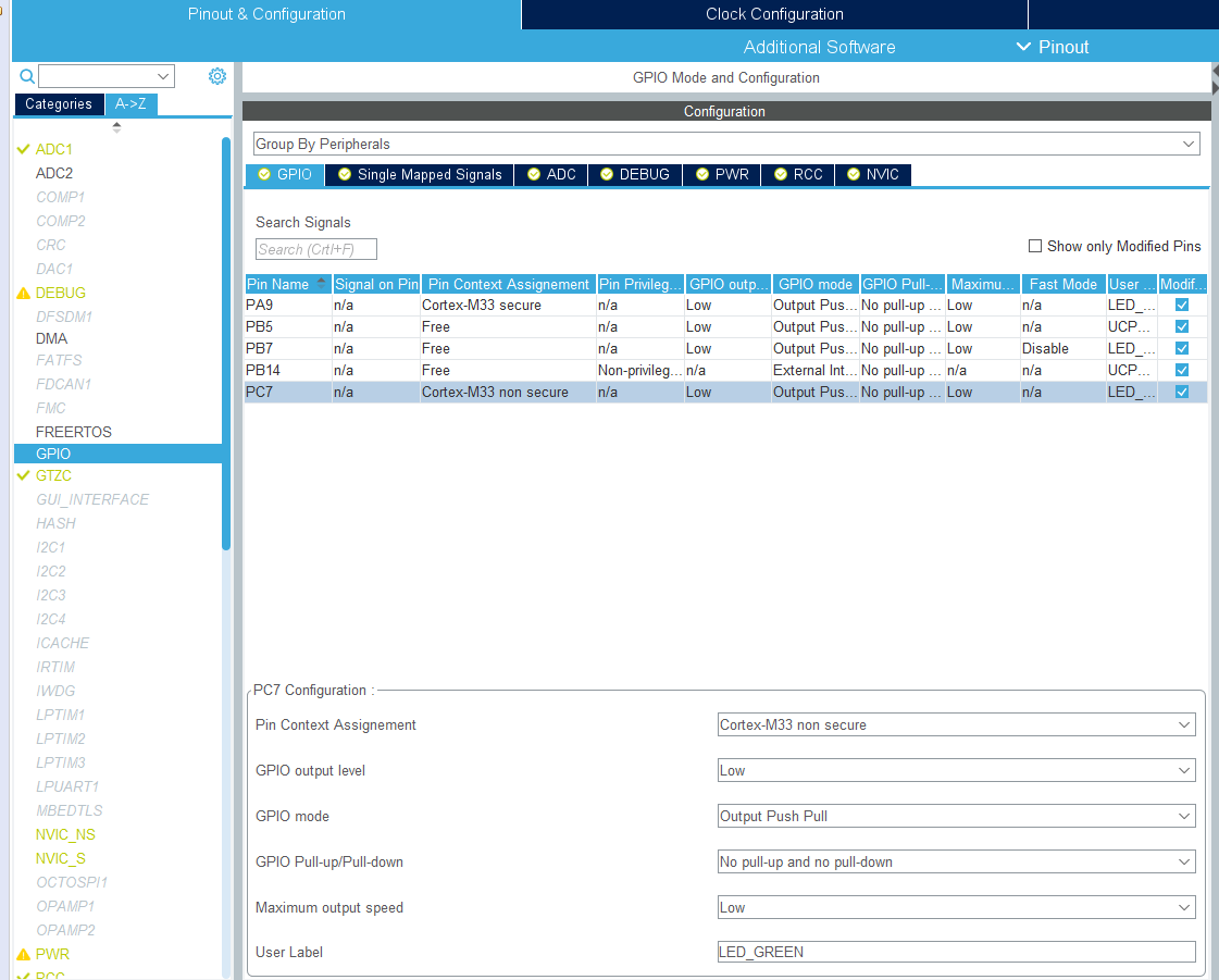
Figure 10.19: Example Project Configuration: GPIO and Peripheral Configuration
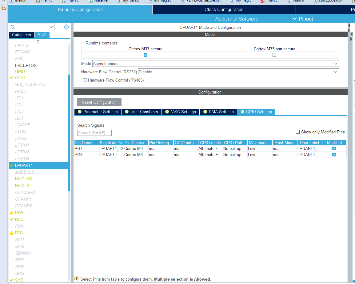
Figure 10.20: Example Project Configuration: GPIO and Peripheral Configuration
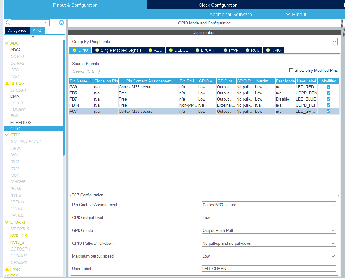
Figure 10.21: Example Project Configuration: GPIO and Peripheral Configuration
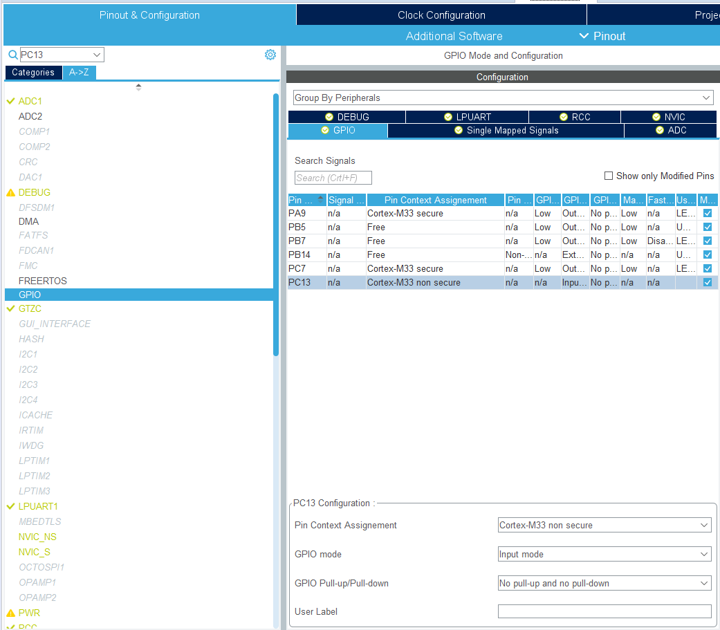
Figure 10.22: Example Project Configuration: GPIO and Peripheral Configuration
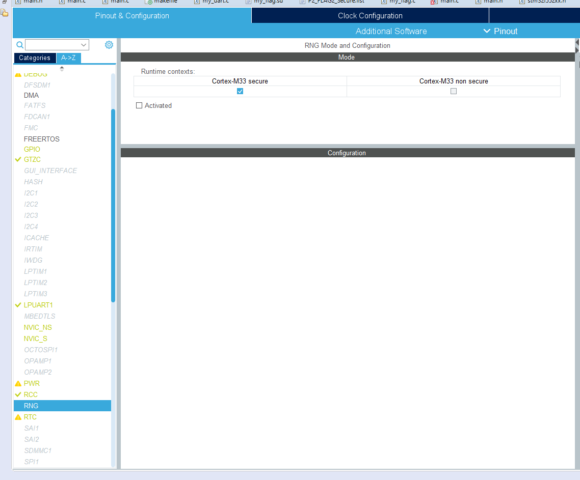
Figure 10.23: Example Project Configuration: GPIO and Peripheral Configuration
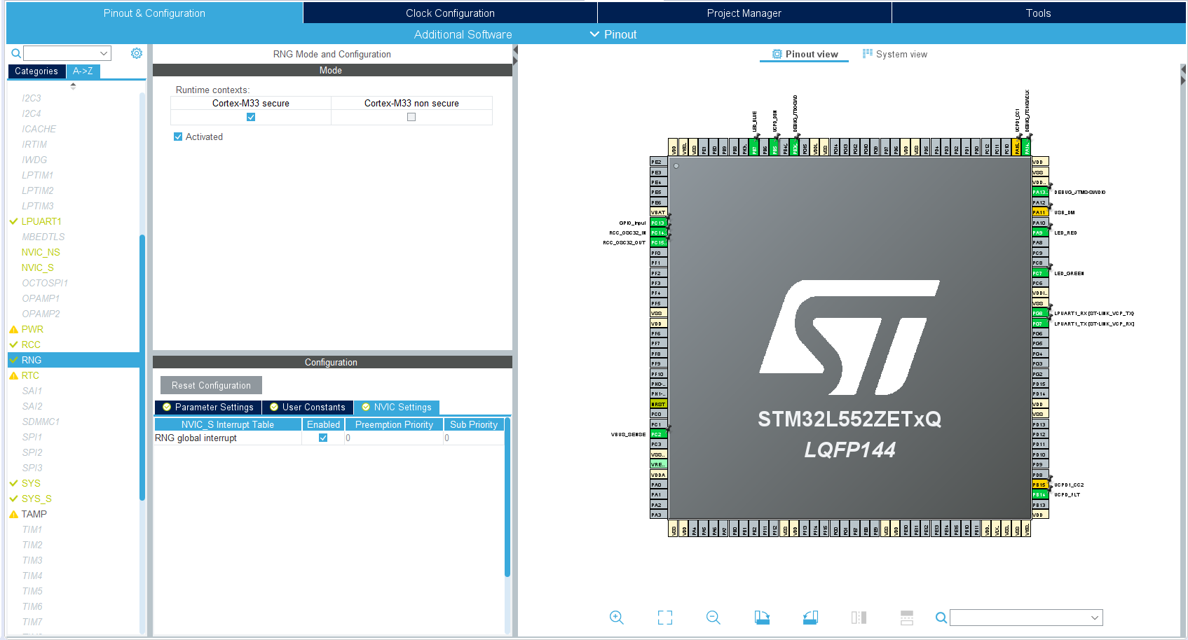
Figure 10.24: Example Project Configuration: GPIO and Peripheral Configuration
10.3.3.1.1.3 Final Project Configuration
Figure 10.25: Example Project Configuration: Final Project Configuration
Figure 10.26: Example Project Configuration: Final Project Configuration